Defects such as cracks in a material can be responsible for the failure of structures as big as the nuclear reactors to the smart phones in our pockets. Now researchers from Georgia Institute of Technology, University of Pittsburg, Sandia National Laboratories and Zhejiang University (China) have discovered a new type of atomic-scale defect, called stacking fault tetrahedron, that can critically affect the deformation and fracture of pressure vessels in nuclear reactors and interconnects in smart phones.
The work is published online in Nature Communicationson August 15, 2013. The team is led by Ting Zhu, an associate professor of Mechanical Engineering at Georgia Tech, and Scott Mao, a Professor of Mechanical Engineering at University of Pittsburg.
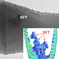
The individual stacking fault is well known and has been studied extensively. However, in 1959, Sir Peter Hirsch and his coworkers at University of Oxford discovered a peculiar defect consisting of four stacking faults that were oriented in different directions but forming an interesting spatial structure of a small tetrahedron. "These stacking fault tetrahedra typically have the size of a few nanometers - approximately 1/50,000th of the width of a human hair," Mao said, "they are only visible under electron microscope, thereby posing a challenge to the study of their origin and evolution in real time."
It has been a mystery as to how a stacking fault tetrahedron is formed. A prevalent hypothesis ascribes its formation to the aggregation of vacancies - missing atoms at regular atomic sites. Vacancies are common in irradiated materials in nuclear reactors and heated interconnects in microchips. "The vacancy-based hypothesis sounds reasonable," said Mao.
Now in the Nature Communications paper, Zhu and his team reported the discovery of an entirely new mechanism of formation of stacking fault tetrahedra. They found that the stacking fault tetrahedra are actually a product of direct interaction of stacking faults formed during mechanical deformation. In other words, vacancies are no longer the pre-requisites for the formation of stacking fault tetrahedra.
The team's discovery is enabled by recent advances in nanotechnology: real-time visualization of atomic-scale dynamic deformation processes using electron microscope, and large scale molecular dynamics simulations in high performance supercomputers. "We observed the deformation-originated stacking fault tetrahedra in a variety of materials such as gold and silver nanocrystals through electron microscope in real time," said Jiangwei Wang, a graduate student at University of Pittsburg. "Our computer simulations were able to capture all the detailed dynamic processes of the formation of stacking fault tetrahedra through stacking fault interactions," said Sankar Narayanan, a graduate student at Georgia Tech. "I give credit to the work ... as an excellent example of the experiment validated by simulation or the simulation validated by experiment," an anonymous referee of the paper commented.
In the Nature Communications paper, the team also reports both the observation and simulation of movements and annihilations of stacking fault tetrahedra during mechanical deformation. These studies demonstrate that the evolution of stacking fault tetrahedra plays an essential role in the deformation and fracture of small-sized nanocrystals. "This work provides a new perspective on how the defects such as stacking fault tetrahedra control the failure in irradiated materials and interconnects," said Zhu.
The ongoing follow-up study by the team indicates that the stacking fault tetrahedra could also be prevalent during the deformation of bulk materials that contain a large number of interfaces, such as nanocrystalline metals. "A further study of the related deformation processes would have broader implications for controlling and optimizing the mechanical properties of nanostructured materials," Mao noted.
The work was supported through the Department of Energy Office of Nuclear Energy’s Nuclear Energy University Programs, National Science Foundation, and Center for Integrated Nanotechnologies, a Department of Energy, Office of Basic Energy Sciences user facility of United States.