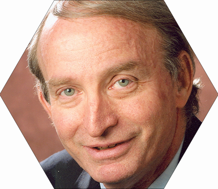
Education
- Ph.D., 1971, Rice University
- B.S., 1967, University of California at Santa Barbara
Background
Dr. Gole began at Tech in 1977 as an Assistant Professor. Prior, he was an Assistant Professor at MIT and a Postdoctoral Fellow at Columbia University.
Research
- Micro and Nano Engineering; Nanostructured materials, porous media, sensors, and micro- and nanocatalysis
Dr. Gole considers the dynamics of complex and cluster formation and reaction-interaction in supersonic gas expansions at highly elevated gas phase concentrations, at the gas-surface interface, and within surface bounds. In physical processes at surfaces, this group is strongly oriented to MEMS applications which include chemical and biosensors, photocatalytic and photovoltaic devices, and micro- and nanobattery configurations. A substantial effort is now channeled into the study of porous (primarily silicon) structures and interfacial phenomena involving these structures.
In collaboration with Professor Peter Hesketh, we are developing highly sensitive chemical sensors using the PS interface. We now have operational chemical and biosensors which have unprecedented sensitivity and response and whose selectivity is being improved with the application of selective coatings and stereolithography generated micro-chromatographs.
In concert with a substantial effort in the development of nanotechnology, we are collaborating with Professor Andrei Federov to develop a photocatalytic microreactor with applications including environmental disinfection and the highly efficient cracking of water.
Semiconductor nanostructures, nanoagglomerates, and nanowires have attracted considerable attention because of their potential applications in mesoscopic research, the development of nanodevices and the potential use of large surface area structures for catalysis.
Following efforts in porous silicon (PS) our research has been extended to the formation and characterization of silicon, silicide, silicon carbide, and tin oxide and doped titanium oxide based nanostructures. Here we have applied the techniques of high temperature synthesis to generate virtually defect free SiO2 sheathed crystalline silicon nanowires and gram quantities of silica (SiO2) nanospheres which can be agglomerated to wire-like configurations impregnated with crystalline silicon nanoclusters.
Finally, the group considers the combination of porous media and selectively generated nanostructures to form novel optoelectronic (photonic) and photovoltaic devices. In collaboration with Professor Bill King we are concerned with the generation of well defined and patterned, monodisperse, nanoporous arrays for combined photonic and photocatalytic applications.
Future applications will lie in the development and application of interfacial arrays incorporated with nanostructures for sensor, catalyst, battery and photovoltaic applications. MEMS and Nanotechnology are both newly developing and wide open areas of endeavor, both of which are successfully engineered using the combination of a great many newly emerging technologies. Students will combine many disciplines including but not limited to microfabrication and microelectronics, kinetics, optical spectroscopy, and the incorporation of these disciplines into the fabrication of devices.
- Georgia Institute of Technology
- Outstanding Undergraduate Research Mentor Award, 2008
- Outstanding Research Author Award, 1990
- Sigma Xi (Georgia Tech Chapter) Sustained Research Award, 1989
- Review of Scientific Instruments Editorial Board, 1984-present
- High Temperature Science Editorial Board, 1979-present
Patents
- Method and Apparatus for Lithiating Alloys, U. S. Patents 6,203,852, with F. P. Dudel, March 20, 2001
- Method and Apparatus for Lithiating Alloys, U. S. Patents 6,010,750, with F. P. Dudel, January 4, 2000
- Purely Chemical Process Yielding Continuous Laser Amplification in the Visible and Ultraviolet Spectral Ranges, U .S. Patent 5,093,182, with S. H. Cobb and J. R. Woodward, March 3, 1992
- Chemical Process Yielding Stimulated Emission of Visible Radiation via Fast Near Resonant Energy Transfer, U. S. Patent 5,050,071, with S. H. Cobb and J. R. Woodward, September 17, 1991
- Chemical Process Yielding Stimulated Emission of Visible Radiation via Fast Near Resonant Energy Transfer, U. S. Patent 5,020,071, with S. H. Cobb and J. R. Woodward, May 28, 1991
- Chemical Process Yielding Stimulated Emission of Visible Radiation via Fast Near Resonant Energy Transfer, U. S. Patent, 4951,297, with S. H. Cobb and J. R. Woodward, August 21, 1990
- Purely chemical Process Yielding Continuous Laser Amplification in the Visible and Ultraviolet Spectral Ranges, U. S. Patent 4,945,546, with S. H. Cobb and J. R. Woodward, July 31, 1990
Representative Publications
- J. L. Gole, L. A. Tse, and P. J. Hesketh. 2002. Rapid, Reversible, and Sensitive Porous Silicon Gas Sensor. Journal of Applied Physics 91, 2519.
- J. L. Gole, et al. 2002. Tin Oxide Nanowires, Nanoribbons, and Nanotubes. Journal of Physical Chemistry B106, 1274-1279.
- J. L. Gole, et al. 2001. Electrochemical Properties of Li-Mg Alloy Electrodes for Lithium Batteries. Journal of Power Sources 92(70), 70-80.
- J. L. Gole, et al. 1997. On the Origin of Porous Silicon Photoluminescence-Evidence for an Oxyhydride-Like Emitter. Physics Review B56, 2173.
- J. L. Gole and D. R. Grantier. 2000. Excited State Mediated Collision Induced Raman Pumping. Molecular Physics 98, 1441.

