Electron Beam Technique Carves and Constructs at the Nanoscale
Georgia Tech researchers demonstrate a new way to sculpt materials with atomic precision, offering new possibilities for electronics, healthcare, and beyond.
July 21, 2025
By Ashley Ritchie
Creating complex structures at the tiniest scales has long been a challenge for engineers. But new research from Georgia Tech shows how electron beams, already widely used in imaging and fabrication, can also be used as ultra-precise tools to both carve and build structures out of materials like copper.
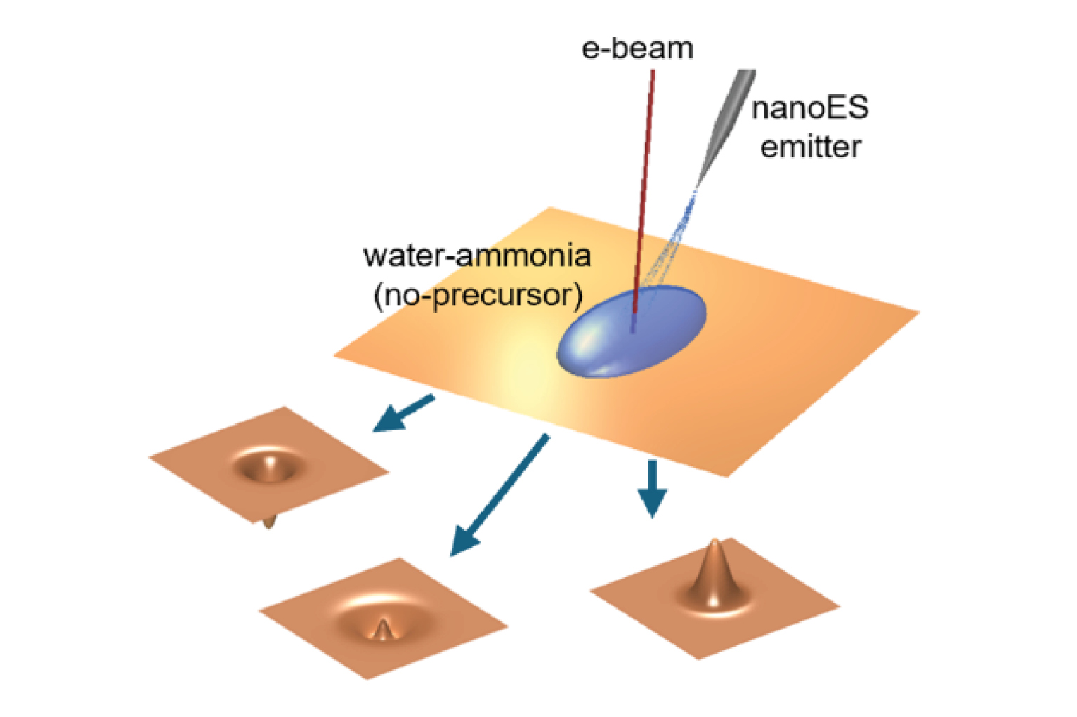
The research group of Professor Andrei Fedorov in the George W. Woodruff School of Mechanical Engineering has discovered a technique that uses focused electron beams in a liquid environment to either remove or deposit copper, depending entirely on the surrounding chemistry. By tuning the amount of ammonia in the solution, the researchers were able to control whether the beam etched away the material or deposited it, effectively allowing 3D sculpting at the atomic level.
Their findings were recently published in the journal Advanced Functional Materials.
A Two-Way Street
Electron beam methods are typically used to remove material or add it, but not both. In this study, the researchers developed a process that can do either, or even both, in sequence, using the same setup.
In experiments, they focused an electron beam on copper submerged in a water-ammonia solution. With low ammonia concentrations, the beam etched narrow trenches just 50 nanometers deep, roughly 2,000 times thinner than a sheet of paper. Over time, copper atoms removed in the etching process began to redeposit inside the trenches, forming tiny vertical structures like peaks inside valleys. By controlling the electron exposure time and number of electrons hitting the material, smaller or larger size patterns and structures could be created.
When the team increased the ammonia concentration, the chemistry changed. The environment became more reducing, which favors the buildup of copper rather than its removal. In this case, the beam acted as a guide, directing where copper was deposited to form intricate nanostructures.
Ammonia as a Switch
The key to this precise control lies in the role ammonia plays in the liquid solution.
“Ammonia does several important things. It helps carry copper atoms in solution, neutralizes unwanted reactions, and makes the environment more favorable for building instead of etching,” said Auwais Ahmed, lead author on the study and Ph.D. student in the Woodruff School.
By carefully adjusting the ammonia concentration and the electron beam exposure, the team was able to fine-tune the shape and structure of the copper surface with nanometer precision. They also developed models and ran simulations to better understand how these chemical changes affect the behavior of the copper.
“What’s exciting is that we’re not just building or removing—we’re dynamically switching between those modes in real time,” Fedorov said.
Tiny Tools for Big Impact
The ability to sculpt surfaces at the atomic level has wide-ranging implications for future technologies. This new method could be used to create ultra-sensitive scientific tools such as microscopic probes and sensors, nanoscale needles for targeted drug or gene delivery, and 3D-stacked wiring in next-generation computer chips.
And because the approach is chemically tunable, it could eventually be applied to other materials beyond copper.
“This gives us a flexible new tool for nanoscale manufacturing,” Ahmed said. “By controlling the local chemistry, we can essentially 3D print and subtract at the same time—opening up new possibilities for design and fabrication in nanotechnology.”